Labtalk Article http://nanotechweb.org/ IOP
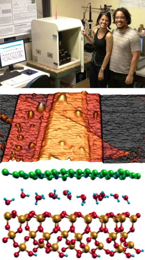
Hexagonal boron nitride (h-BN) is well suited as a substrate to form ultra-fast transistors with graphene. In many examples and prototypes that have been reported, h-BN layers are mechanically exfoliated onto silicon oxide supporting substrates. In a subsequent step, graphene layers are laid on the h-BN layer, which enables the fast carrier transport in graphene. Now, researchers at Universidade Federal de Minas Gerais, Brazil, have studied the influence of trapped water nano-ponds on the properties of such h-BN layers.
See More: http://iopscience.iop.org/0957-4484/labtalk-article/49398

The main researchers behind this work, Camilla Oliveira (experiments) and Matheus Matos (simulations) in the SPM lab, which is located in the Physics Department of Universidade Federal de Minas Gerais. (b) AFM image of a typical sample of few-layer h-BN (in orange-brown shades) mechanically exfoliated onto a silicon oxide substrate (in gray). Under ambient preparation conditions, a water film is confined between h-BN and the silicon oxide. (c) A snapshot of the theoretical simulation, showing water molecules (red/blue) sandwiched between h-BN (green/blue) and the silicon oxide (yellow/red).
